Please update your browser.

It looks like you are using an old version of the Microsoft Edge browser. To get the best experience with the Busch website, please update your browser.

Contact
Global
  • EN
  • DE
  • FR
  • ES

Solar Cell Manufacturing With Vacuum

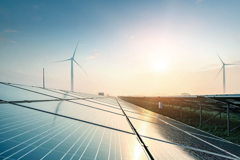
By utilizing cutting-edge vacuum technology, manufacturers can produce solar panels at a faster rate and increase the panels’ efficiency and durability.

solar_panels

The role of vacuum in solar cell manufacturing

The solar industry is paving the way for renewable energy sources of the future. Vacuum plays a key role in future-proofing solar panel manufacturing. It is used from the first moment to create the silicon that makes up each cell, right up to laminating the final layers together.

Solar panels are a popular choice for consumers and businesses as the technology becomes more efficient and cost-effective. However, as the demand for solar panels continues to grow, so does the need for more efficient production processes.
Vacuum allows faster production and increased efficiency and durability of solar panels.

By utilizing cutting-edge vacuum technology, manufacturers can produce solar panels at a faster rate and increase the panels’ efficiency and durability.

Additionally, optimal vacuum technology can also help reduce waste and increase the sustainability of the solar panel production process. Less material is wasted by ensuring that coatings are distributed evenly onto the solar cells.

Busch offers optimal vacuum solutions for the solar power industry.
Vacuum applications in manufacturing solar cells

By using vacuum technology, solar panel manufacturers can produce durable, efficient, and reliable solar panels.

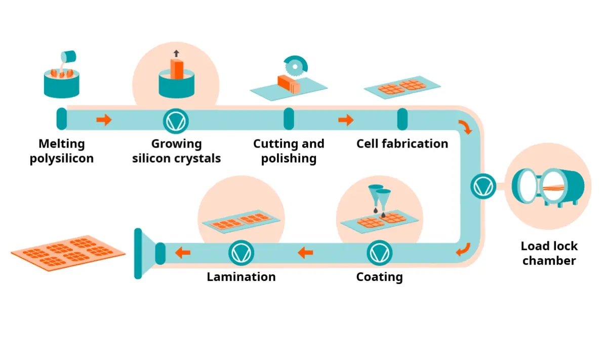
There are four main vacuum applications during the solar panel manufacturing process:
solar_panel_production_infographic_ingot

Growing silicon crystals under vacuum

The cells that make up a solar panel are made of silicon, one of the most abundant elements on Earth. It is found in almost all rocks, natural beach sands and soils, but always in combination with other elements – usually oxygen.

Pure silicon is needed for solar panels. To create it, polysilicon, a high-purity form of silicon, is melted, and a seed crystal is introduced. However, in its melted state, silicon becomes especially reactive. Gas molecules, dust particles, and other impurities can react and interfere with the growth of silicon crystals, ultimately affecting their performance and the efficiency of the solar panel.

A vacuum system is used to extract all air from the process chamber. Under vacuum, the silicon no longer has anything to react with, so the crystal will be free of impurities.

In this contaminant-free environment, the pure silicon can be grown. It starts to form on the seed crystal. As the crystal is slowly pulled out of the molten silicon, it creates one long rod that can sliced into ultra-thin wafers of around 200 µm.

However, certain impurities are necessary. Doping introduces miniscule amounts of another element, usually boron or phosphorous, to create the silicon wafer. These bond with the silicon atoms and create “free electrons” that can transmit electricity across the circuit. This is what changes pure silicon, an insulator, into a semiconductor.
solar_cell_manufacturing_load_lock_chambers

Load lock chambers

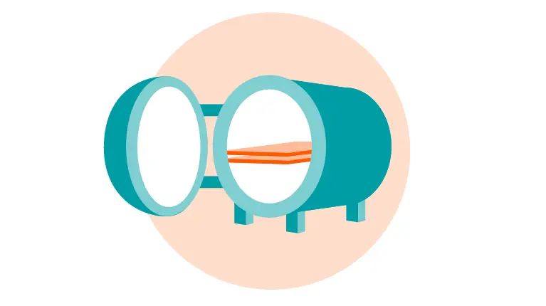
Several critical stages of solar panel production take place in a vacuum chamber in order to provide a stable, contaminant-free environment for the sensitive silicon wafers.

However, to avoid sudden changes in pressure when transferring the wafers from atmospheric conditions to the main chamber, an intermediary stage – the load lock chamber – is necessary. It fulfils a similar role to an air lock on the door of a space craft, providing a buffer between the two chambers when wafers are loaded and unloaded.

The load lock chamber is cycled between atmospheric ambient pressure and the vacuum level in the main chamber. This means that the main chamber never loses pressure, ensuring fast cycle times and reduced contamination.

Matching Products for load lock chambers
solar_panel_production_infographic_coating

Coating processes

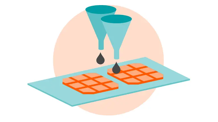
Solar cells are coated with different materials. Depending on the material and the technique, the coating has different properties. Using vacuum ensures that the coating material is distributed evenly, is free of air bubbles, and has uniform thickness. All of which enhance each solar cell’s efficiency.

There are two different coating methods used in solar panel manufacturing: physical vapor deposition (PVD) and plasma-enhanced chemical vapor deposition (PECVD). These are both thin-film deposition techniques but have different methods and are used for different purposes. In a PVD process, the vapor condenses on the substrate to form the coating. The PECVD process, however, causes the vapor to undergo a chemical reaction on the substrate, creating a thin film.

In solar panel manufacturing, PVD is typically used to add a physical layer, such as a protective layer to shield the solar cell from the elements.

Matching products for PVD coating

On the other hand, PECVD is used when specific chemical and electrical properties are required, such as adding a layer of anti-reflective coating. This makes the solar panel more efficient by helping the cells capture light particles to generate electricity.Find out more about how coating processes work.

Matching products for PECVD coating
solar_panel_production_infographic_lamination

Lamination of solar modules

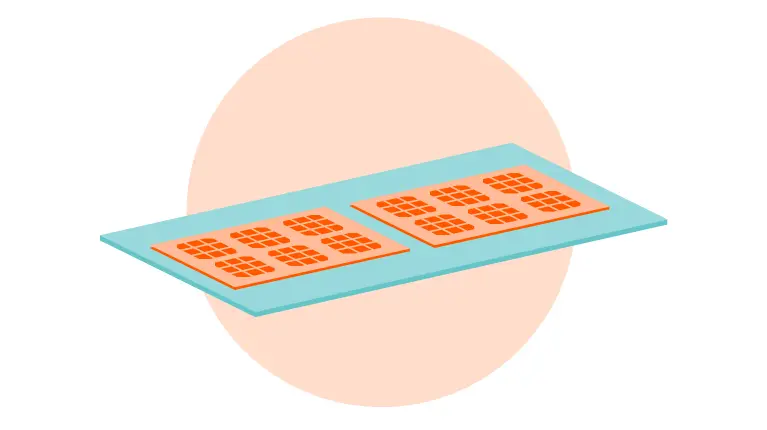
High-quality lamination is crucial to ensure the longevity of solar modules. Several layers of wafers are bonded during this process, including a glass cover and protective backing sheet.

Vacuum removes any trapped air between the layers, creating a tight bond and eliminating the risk of delamination, which could decrease the solar module’s efficiency over time.

Matching Products for lamination

Need vacuum in your process?

We will design your tailor-made vacuum solution.

Our matching products

Our vacuum solutions are operated at major solar panel production sites. The world over. And are renowned for their reliability. In all stages of solar panel production.

 
PVD coating
CVD/PECVD coating
Lamination
Load lock chamber
 
COBRA NX
PANDA WV

(load lock chamber)
 
 
COBRA NX
PUMA WY

(process chamber)
 
 
COBRA DS

(load lock chamber / process chamber)
COBRA NC
PANDA WV


(first chamber)
COBRA NX
PANDA WV


(second chamber)
MINK MM


COBRA NX
PANDA WV


Learn more about solar cell manufacturing with vacuum

What is the difference between a solar cell and a solar panel?

When we talk about solar energy, we tend to talk about solar panels. But a solar panel is not the smallest component. The smallest is the solar cell, or photovoltaic cell. It comprises two layers of semiconductor wafers. When multiple solar cells are wired in parallel, they make up a solar module. These are encapsulated and sealed as one object.

One or more solar modules packaged as an installable unit become a solar panel. And a solar array consists of multiple solar panels wired in series or parallel – as small as just a few modules or over several hectares.

How are solar panels manufactured?

The manufacturing process of solar panels, also known as photovoltaic (PV) panels, is composed of several steps, including the production of silicon wafers, cell processing, and module assembly.

The most common solar panel manufacturing process includes the following three vacuum applications:

  • Growing silicon crystals: Quartz sand (SiO2) is heated at high temperatures with a reducing agent (carbon) in a furnace. The oxygen molecules in the sand combine with the carbon to create carbon monoxide (CO), leaving pure molten silicon behind. A seed crystal rod is placed on the silicon surface and slowly pulled up. This action combined with rotation forms a silicon ingot. To avoid impurities entering the silicon crystal, this process takes place under vacuum. Then, the silicon ingot is sliced into paper-thin disks called silicon wafers.
  • Coating processes: Depending on the type of solar panel being manufactured, silicon wafers undergo various chemical processes before they are fabricated into solar cells. As pure silicon is shiny, the cells are reflective. Thus, an anti-reflective coating is deposited on their surface under vacuum.
  • Lamination of solar modules: Several solar cells are joined together via metal connectors to form a solar module. A thin layer of glass is placed on top of the module, and the back sheet is made of a highly durable, polymer-based material. Vacuum ensures that any trapped air between the layers is removed, ensuring the strength and longevity of the finished module.

Are there different types of solar panels?

There are four main types of solar panels:

  • Monocrystalline panels, also known as single-crystalpanels, are made by growing a single pure silicon crystal that is cut into multiple wafers. They are ideal for locations with limited space. Even in areas with little sunlight, these solar panels are able to collect the maximum amount of energy.
  • Passivated emitter and rear cell panels (PERC) are a modified version of monocrystalline panels with increased efficiency. They have an additional reflective layer on the back. This enables them to capture extra photons and produce more solar energy than a traditional panel.
  • Polycrystalline or multicrystallinesolar panels are made up of several silicon crystals. Wafers are formed by melting together a number of silicon fragments. This mixture is then poured into a mold the size of a single solar cell. This makes polycrystalline panels more eco-friendly, as their forming process means that little to no material goes to waste. Within this category, a distinction can be made between the following two types:
    • Tunnel oxide passivated contact (TOPCon): On the rear side of the cell, an ultra-thin oxide layer is added. This helps the cell handle higher voltages, increasing power production. TOPCon cells are also more efficient than PERC cells, especially in lower light conditions.
    • Heterojunction (HJT): These cells are made up of three layers of photovoltaic material. They use two different cell technologies, polycrystalline silicon and thin-film silicon, which work together to produce electricity. HJT cells are generally combined to create bigger panels than other cell technologies and can reach high efficiency levels.
  • Thin filmsolar panels are made of several layers. These layers are so thin that they are flexible. The panels are lighter and easier to install as they do not require a frame backing. Thin-film solar panels are not made of silicon but of cadmium telluride (CdTe), amorphous silicon (a-Si), and copper indium gallium selenide (CIGS), also known as perovskite. They are more efficient than HJT cells.

Each type of solar panel uses vacuum at varying stages of the solar panel manufacturing process. Depending on the type, this may be during silicon growing, coating, or laminating, or all three.

What is the raw material for solar panel manufacturing?

Quartz sand, also known as natural beach sand, is used to manufacture solar panels. From this sand, pure silicon can be produced, which is the main material necessary in solar panel manufacturing. Pure silicon is extremely reactive in its molten state, so it is processed under vacuum to avoid impurities entering the silicon crystal.